GameTank Motherboard
System bus and memory map
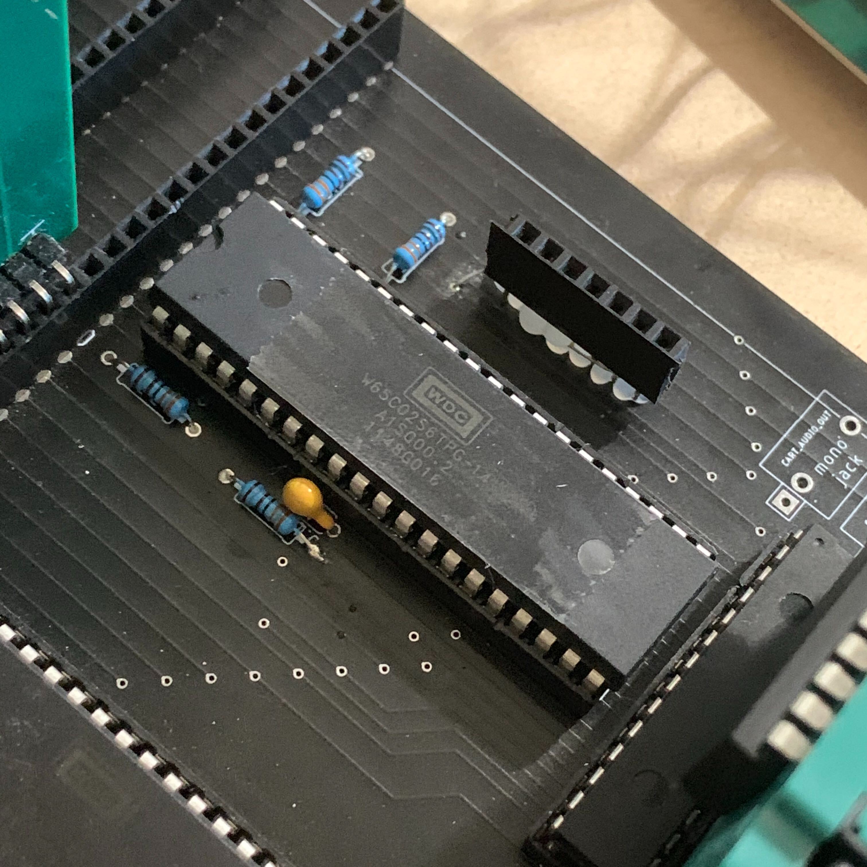
The GameTank's motherboard is home to the 6502 CPU, the 6522 Versatile Interface Adapter, some general-purpose Random Access Memory, the cartridge port, and a smattering of glue logic that defines the memory map as well as shapes the timing of certain control signals. The motherboard, in a sense, bookends the project by featuring the earliest design decision while being the last piece implemented. One of the first choices I'd made for the GameTank would be the use of the 6502 as the CPU. Then I bought one on eBay, put it in a drawer, and promptly forgot about it as I went off to play with composite video.
The first tests for the video, DMA, and audio boards either used an Arduino to emulate the system bus or simply read data directly off an EEPROM chip. In many ways this actually turned out to be a good idea. There is a wealth of information available on building 6502-based retrocomputers, while the design for the peripherals had many unanswered questions. Once I had fleshed out the I/O devices I had a pretty good idea of the requirements for driving these subsystems, and thus how I should draw up the memory map.
The 6502 is a remarkably simple device to interface digital logic with. At each cycle the sixteen address pins output a binary number between 0 and 65535, along with a read/write signal that specifies whether a read or a write is being performed. If a write is being performed, then eight data pins will output a binary number between 0 and 255. Otherwise the data pins will act as inputs to receive a binary number from some other device. The system designer can then use any logic they like to interpret the value from the address pins to decide which other device should now accept input from the data pins (during a write) or output their own value to the data lines (during a read). A scheme for assigning addess values to peripheral devices is called a memory map.
The only rules for a 6502 memory map are that the first 512 addresses should be RAM and the last 6 addresses are typically ROM. Page 1, or the memory range between 256-511, holds the stack. The stack is a first-in last-out data structure where you can "push" values onto the stack or "pop" them off in the reverse order that you pushed them. Several opcodes can be used for pushes and pops directly, but the other major use of this memory is for subroutines and interrupts. When a subroutine is called or an interrupt handler is triggered, the address to return to is pushed onto the stack and then popped back off when the subroutine completes. Without RAM in Page 1, the software cannot make use of subroutines or interrupts. There are also several opcodes that only work on page 0 (addressses 0-255) in exchange for having to specify one fewer byte in the instruction. Finally, the last 6 addresses tell the CPU where to start executing code when an interrupt is triggered or a system reset has completed. If these values are not available when the system powers on, then the system will not behave predictably or even be particularly useful.
Rather than arbitrarily pick ranges of numbers to assign, it is typically easiest to work in halves. Starting from the highest bits of the address value, a memory map can be designed as a sort of binary tree where each branch is a choice between two paths. This lends itself well to digital circuit design, as logic gates can be arranged to form branches indepentently of each other. This is why address ranges in a memory map may tend towards power-of-two lengths.
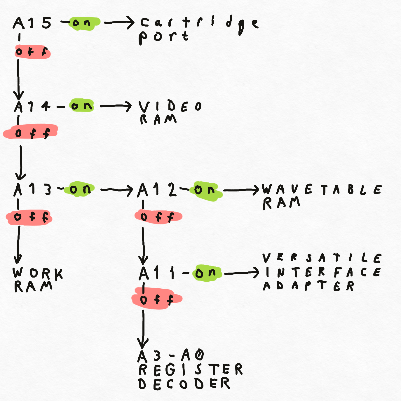
The GameTank memory map follows these recommendations and is laid out as follows:
- Pages 128-255 are directed to the cartridge port, which primarily hosts a ROM chip.
- Pages 64-127 are mapped to the Video DMA board, which exposes either V.RAM, G.RAM, or its own control registers.
- Pages 48-64 are mapped to the RAM chip hosted on the audio board, which holds the sample data for the wavetable channel.
- Pages 40-47 all map to the 6522 VIA chip, it's just the same 16 register mappings repeated. There isn't much reason to use addresses outside of $2800-$28OF.
- Pages 32-39 map to the same eight control registers on repeat, but similarly there's not much reason to use the addresses outside of $2000-$2007. Addresses $2000-$2006 control the audio hardware while $2007 holds certain graphics control flags.
- Pages 0-31 map to general purpose RAM, which holds the stack I mentioned earler as well as space for any variables and arrays the programmer wishes to use.
The first version of the GameTank motherboard was designed as a backplane. The address/data bus and control signals are exposed via rows of headers that peripherals could plug into, much like expansion cards for a desktop PC. In addition, certain device-select signals generated by the memory map logic were exposed on headers that could be connected to different devices by jumper wires. While this turned out to be somewhat useful for experimenting, it does mean that the assembled V1 prototype is a rather fragile jumble of wires. For this reason the new motherboard design replaces the jumper wires with dedicated pins on the board-to-board connectors, making the memory map arrangement permanently configured.
Finally, the 6522 Versatile Interface Adapter (or just "VIA") adds two features to the system. One is a programmable counter that can generate an interrupt after a certain number of cycles. The other is a pair of bidirectional I/O ports which have been wired to access SPI hardware on the cartridge as well as an array of LEDs that will go on the front of the console. Well, on the V1 motherboard the VIA was wired to use the I2C serial protocol, but on V2 this has been replaced with a more straightforward SPI port. Serial EEPROM chips are cheaper than the parallel EEPROM chips that store the program on a basic GameTank cartridge, and are available with higher capacity. The tradeoff is that the CPU can't directly access this memory to execute instructions, so some more work has to be performed to access this data. It is ideal for storing compressed graphics which can be extracted to Graphics RAM during a loading screen, and then don't need to be accessed directly off of the SPI very often after that.